
Listen to this Post
Introduction:
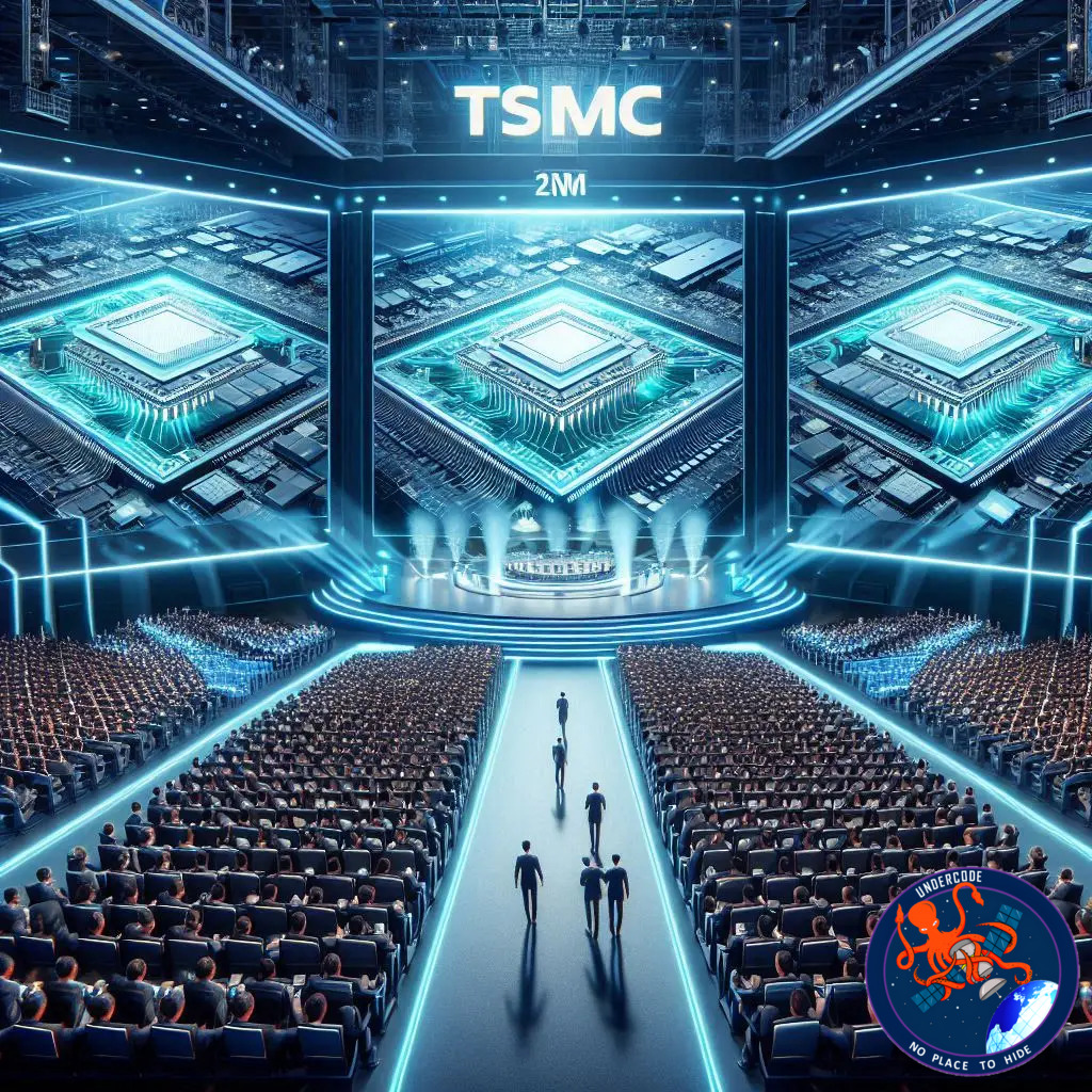
Taiwan Semiconductor Manufacturing Company (TSMC), the world’s largest contract chipmaker, has officially begun mass production of its 2-nanometer (nm) chips, setting a new benchmark in semiconductor innovation. This development not only highlights TSMC’s technological leadership but also signals a major leap in performance, energy efficiency, and computing density that will power the next generation of devices—from AI servers to flagship smartphones.
TSMC’s 2nm Chips: A New Frontier in Performance and Efficiency
TSMC’s announcement marks the commercial rollout of its most advanced process node yet. The 2nm chips are designed to deliver higher performance compared to the 3nm generation while maintaining lower power consumption, a crucial factor for mobile devices, AI workloads, and high-performance computing. The reduced transistor size allows for denser, more powerful chip designs, opening doors for smaller yet more capable electronic devices.
Mass production is already underway at TSMC’s Hsinchu and Baoshan facilities in Taiwan, with plans to scale up output in the coming year. The new 2nm chips are expected to power next-generation iPhones and advanced AI servers, reinforcing TSMC’s position at the forefront of chip innovation.
TSMC is also pursuing global diversification by building new fabs in Arizona, Japan, and Germany. This strategic expansion aims to mitigate geopolitical risks while meeting growing worldwide demand for advanced semiconductor technologies.
The timing of this launch is critical. Demand for AI accelerators, smartphones, and high-performance computing solutions is surging globally, and TSMC’s 2nm chips position the company ahead of competitors such as Samsung Electronics and Intel, both of whom are racing to develop similar next-generation nodes.
Nvidia CEO Jensen Huang praised TSMC for its role in supporting Nvidia’s chip production, emphasizing that Nvidia’s success depends heavily on TSMC’s wafer manufacturing capabilities. Huang also noted the strong demand for Nvidia’s Blackwell chips, highlighting the increasing need for advanced GPUs, CPUs, and networking components powered by cutting-edge semiconductor nodes.
What Undercode Say:
TSMC’s launch of 2nm chips is a pivotal moment that underscores several critical trends shaping the semiconductor landscape. Firstly, the shift to smaller nodes is no longer just a technical milestone; it is a strategic differentiator. The reduction to 2nm enables more transistors per square millimeter, translating to higher computing power, greater energy efficiency, and lower heat generation. This is particularly important for AI workloads, which demand both raw computational capacity and energy optimization.
Secondly, TSMC’s aggressive global expansion highlights a deliberate strategy to reduce geopolitical exposure. By establishing fabs in the U.S., Japan, and Germany, TSMC is not only diversifying its supply chain but also strengthening its influence over the next-generation semiconductor ecosystem. These moves reflect broader industry concerns about supply chain security, national technology sovereignty, and the escalating competition between East and West over semiconductor dominance.
From a competitive standpoint, TSMC’s 2nm chips provide a temporary but significant lead over Samsung and Intel. While both rivals are actively developing smaller nodes, TSMC’s early production and proven reliability in high-volume manufacturing provide a clear market advantage. The ability to supply chips at scale for smartphones, AI servers, and HPC devices will likely cement TSMC’s market share, reinforcing the company’s status as the indispensable partner for major technology firms like Nvidia, Apple, and AMD.
The collaboration with Nvidia further highlights TSMC’s ecosystem strength. Nvidia’s GPUs and CPUs demand cutting-edge fabrication, and TSMC’s 2nm node enables innovations in Blackwell chips that can handle more complex workloads while maintaining efficiency. This synergy between chip designer and manufacturer underscores the increasing interdependence of semiconductor innovation and production.
Looking ahead, TSMC’s 2nm technology could accelerate breakthroughs in AI, autonomous systems, and mobile computing. Smaller, more efficient chips can drive longer battery life, faster data processing, and more compact device designs, impacting industries from consumer electronics to cloud computing. The 2nm node is not just an incremental improvement—it is a foundation for a decade of next-generation computing innovations.
Finally, TSMC’s continued investment in R&D, fabrication capacity, and global diversification demonstrates a long-term vision that balances technological ambition with market and geopolitical realities. The company’s leadership in node advancement, paired with strategic expansion, ensures that it remains at the center of the global semiconductor supply chain for years to come.
Fact Checker Results:
✅ TSMC has started mass production of 2nm chips.
✅ Production is occurring at Hsinchu and Baoshan facilities in Taiwan.
❌ No official confirmation yet on specific consumer devices using 2nm chips.
Prediction:
📊 TSMC’s 2nm chips are likely to dominate next-generation AI servers, high-performance computing, and premium smartphones over the next 3–5 years.
📊 Nvidia and Apple may leverage 2nm technology to deliver unprecedented performance gains in GPUs and mobile processors.
📊 TSMC’s global fab expansion could reshape the semiconductor supply chain, reducing reliance on a single region and mitigating geopolitical risks.
▶️ Related Video (78% Match):
🕵️📝✔️Let’s dive deep and fact‑check.
References:
Reported By: timesofindia.indiatimes.com
Extra Source Hub (Possible Sources for article):
https://www.linkedin.com
Wikipedia
OpenAi & Undercode AI
Image Source:
Unsplash
Undercode AI DI v2
Bing
🔐JOIN OUR CYBER WORLD [ CVE News • HackMonitor • UndercodeNews ]
📢 Follow UndercodeNews & Stay Tuned:
𝕏 formerly Twitter 🐦 | @ Threads | 🔗 Linkedin | 🦋BlueSky | 🐘Mastodon


