
Listen to this Post
A Strategic Technological Milestone
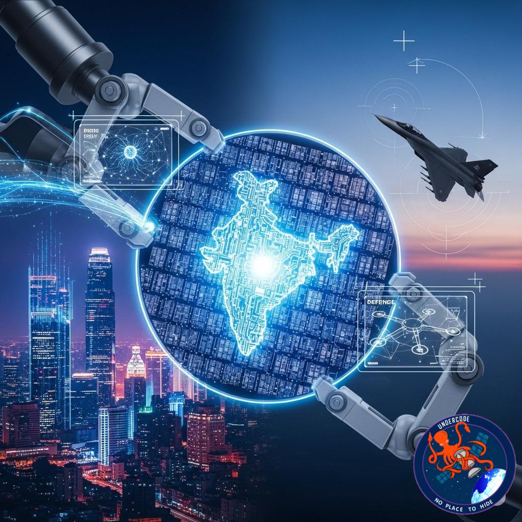
India has taken another decisive step toward becoming a global semiconductor powerhouse. In a move that could reshape the nation’s electronics and high-tech manufacturing landscape, the Union Cabinet, led by Prime Minister Narendra Modi, has approved four cutting-edge semiconductor projects worth ₹4,594 crore under the India Semiconductor Mission (ISM). These projects are strategically spread across Odisha, Punjab, and Andhra Pradesh, with each facility tailored to strengthen capabilities in defence systems, artificial intelligence, automotive technology, renewable energy, and advanced computing. This latest decision raises the total number of approved semiconductor projects under ISM to 10, representing an unprecedented cumulative investment of ₹1.60 lakh crore in six states.
National Scale Expansion of Semiconductor Manufacturing
The four approved proposals come from industry leaders and global collaborators: SiCSem, Continental Device India Pvt Ltd (CDIL), 3D Glass Solutions Inc., and Advanced System in Package (ASIP) Technologies. Together, these ventures are expected to create direct employment for 2,034 highly skilled professionals, while also triggering thousands of indirect jobs in the electronics ecosystem.
Regional Distribution and Key Projects
SiCSem (Odisha) is partnering with UK-based Clas-SiC Wafer Fab Ltd. to build India’s first commercial silicon carbide-based compound semiconductor fabrication facility. With a capacity of 60,000 wafers annually and 96 million packaged units, it will focus on devices vital for defence equipment, missiles, electric vehicles, railways, fast chargers, solar inverters, and consumer electronics.
3D Glass Solutions Inc. (Odisha) will establish a vertically integrated advanced packaging and embedded glass substrate facility. This high-tech plant will produce glass interposers, silicon bridges, and 3D heterogeneous integration (3DHI) modules, delivering about 69,600 glass panel substrates and 50 million assembled units yearly. The output will cater to defence, AI, RF communications, photonics, and high-performance computing.
ASIP Technologies (Andhra Pradesh) will operate in collaboration with South Korea’s APACT Co. Ltd., manufacturing 96 million units annually for use in smartphones, set-top boxes, automotive electronics, and other consumer devices.
Continental Device India Ltd (Punjab) will expand its Mohali plant to produce high-power semiconductor devices such as MOSFETs, IGBTs, and Schottky bypass diodes, with an annual capacity of 158.38 million units for EVs, renewable energy, industrial applications, and communication infrastructure.
Driving Talent Development and Domestic Capability
These developments align with India’s larger strategy to complement domestic chip design expertise, supported by government-backed infrastructure at 278 academic institutions and 72 start-ups. With over 60,000 students trained under national talent development programs, India is not just building semiconductor plants—it is nurturing the brains that will power them.
What Undercode Say:
India’s latest semiconductor push reflects a calculated geopolitical and economic strategy. By spreading projects across multiple states, the government ensures regional industrial balance and maximizes political and economic impact. The integration of foreign partnerships—whether through UK-based Clas-SiC Wafer Fab Ltd. or South Korea’s APACT Co. Ltd.—is a deliberate move to bring in proprietary know-how that domestic firms still lack.
From a technological perspective, this investment is not merely about chip production; it’s about establishing end-to-end capability in compound semiconductors, advanced packaging, and high-power devices. The focus on silicon carbide (SiC) technology is significant—SiC components excel in high-voltage, high-efficiency applications, making them essential for EV powertrains, renewable energy inverters, and advanced defence electronics. This suggests India is aiming not just to participate in global semiconductor supply chains but to dominate niche, high-value segments.
The Odisha projects, particularly the 3D Glass Solutions plant, indicate a push toward next-generation packaging technologies like 3DHI, which are crucial for miniaturized, high-performance systems. This could give India an edge in AI servers, aerospace applications, and 5G infrastructure, where space efficiency and thermal management are critical.
The ASIP facility in Andhra Pradesh adds another layer by targeting consumer and automotive electronics. This diversification of output ensures India does not overly depend on a single segment, making the semiconductor ecosystem more resilient to global market fluctuations. Meanwhile, CDIL’s Mohali expansion will strengthen domestic production of discrete devices—components that, while less glamorous than AI processors, are indispensable in every electronic system.
The employment potential is also noteworthy. Although the direct figure of 2,034 skilled jobs seems modest compared to the investment size, semiconductor facilities are known to generate extensive supply chain employment—from equipment maintenance to logistics and chemical production. The real multiplier effect will be felt across allied industries, including PCB manufacturing, battery systems, and communication networks.
Politically, the move ties neatly into India’s Atmanirbhar Bharat (self-reliant India) vision. By strategically reducing dependency on imports from countries like China and Taiwan, India is seeking both economic sovereignty and a stronger geopolitical bargaining position. The investment also arrives at a time when Western nations are actively seeking alternative semiconductor supply chains to diversify away from East Asia.
However, challenges remain. Semiconductor fabrication is capital-intensive, technology-sensitive, and requires stable power, water, and cleanroom environments. The success of these projects will depend on India’s ability to maintain uninterrupted infrastructure and meet strict global quality standards. Additionally, nurturing a pipeline of engineers with the specialized skills needed for such facilities will require sustained academic and industrial collaboration.
In essence, this decision could be a game-changer for India’s electronics sector—if execution matches ambition. The next three to five years will be critical in determining whether India becomes a credible player in the global semiconductor race or simply a promising but delayed contender.
🔍 Fact Checker Results:
✅ ₹4,594 crore investment figure verified from official Cabinet release.
✅ Locations and company names match approved ISM project list.
✅ Employment projections align with industry standards for semiconductor fabs.
📊 Prediction:
India’s semiconductor ecosystem is likely to see accelerated growth over the next five years, with Odisha emerging as a national hub for compound semiconductor and advanced packaging technology. If the infrastructure and talent pipeline remain on track, India could secure a top-five position globally in niche semiconductor manufacturing by 2030, potentially challenging traditional Asian dominance.
🕵️📝✔️Let’s dive deep and fact‑check.
References:
Reported By: zeenews.india.com
Extra Source Hub:
https://www.reddit.com/r/AskReddit
Wikipedia
OpenAi & Undercode AI
Image Source:
Unsplash
Undercode AI DI v2
🔐JOIN OUR CYBER WORLD [ CVE News • HackMonitor • UndercodeNews ]
📢 Follow UndercodeNews & Stay Tuned:
𝕏 formerly Twitter 🐦 | @ Threads | 🔗 Linkedin | 🦋BlueSky | 🐘Mastodon


